Software to use
The most important thing for designing circuits is having the right CAD program. I use Altium for the board designs. Altium is not a free software, but it is worth the price. For the education licenses, we pay about $5000 a year for 10 floating licenses. Altium is used commonly in the industry. Also, it allows easy integration with mechanical systems as 3D files of the board can be exported. It allows to easily create multilayer boards. Eagle is a popular and free board design software. It works ok for simple designs, but requires buying a license to do multilayer designs.
Component sizes
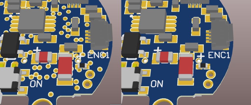
I avoid using any through hole components. It is actually faster to solder surface mount parts.
For passive components (resistors, capacitors, LEDs), I use 0402 and 0603 packages. The 0402 is difficult to solder by hand. The best way is to use a manual pick and place machine. A harder way is to use tweezers and a stencil. The 0603 is easier to solder by hand, but it’s larger, so I would use it for parts that might need to be replaced.
For chips (ICs), I prefer using TQFN packages. They have leads sticking out on the side. This provides two benefits: First, if something needs to be rewired thin wires can be soldered directly to the chip. Second, the chip can be soldered by hand without a stencil Another common package to use is QFN. Those packages don’t have lead sticking out, and therefore they are smaller. They are almost impossible to solder without a stencil and almost impossible to solder wires to. I avoid using BGA packages. They have the connections underneath the chip. Those are impossible to inspect, without an X-ray machine.
Vias
Vias are the holes that connect to from bottom to the top layer. I usually use the smallest hole size that the manufacturer can make (Usually around 8mil diameter). The hole also needs to have an annual ring around it (typically 18mil diameter). It is just a ring of copper plated around the via. This is how the via connects from the bottom to the top layer. There isn’t much reason to use larger vias, as they don’t have much effect anyway in the low power electronics.
The vias should be tented with solder mask on the top and bottom. This means that they will be covered with non-conductive material. It prevents possible shorts and the board will look nicer. On the downside, it is much harder to solder to vias with soldermask, if they need reworking. Typically small vias are too tiny to solder to anyways.
When space is tight vias can be places directly on the pads of components. This works especially well for resistors and capacitors. It doesn’t really have much of an effect on soldering
Trace sizes
Mainly, the wider traces have lower resistance and thus can carry more current without significant voltage drops. I usually use the smallest width of 5mil for signal traces. This can be digital communications or even analog signals. SWuch signals usually carry very little current, and thinner traces reduce parasitic capacitance. For power and ground, I try to make the traces as wide as possible. Something around 10 mil or higher is preferred.
Layers
4-layers boards are preferred for complex designs. Almost anything can be routed on a 4-layer board.
I usually keep one middle layer as solid ground. This makes it easy to connect to ground by simply placing vias anywhere.
Silk screen
I usually don’t put any component designators. They just don’t fit on the board, and they make it more confusing.
The designators can be placed in a mechanical layer. This document can be printed out and followed during the assembly, which is easier than trying to match designators on the board.
Design for easy assembly
The boards will eventually need to be assembled in a factory or in-house. This should be considered during the design process.
For small boards, it is good to ask the manufacturer to penalize them. I usually do 3×3 panel of boards. This allows assembling and testing of 9 boards together, instead of just one. For complex small boards, hand assembly yield might be as low as 20%, so it always makes sense to make more than one board. Also, small boards are hard to handle if they come individually, as they are hard to pick up and hold in place
Design for mistakes
With the first iteration, there are always mistakes. you will probably need to add jumpers or cut some traces. To save time it is good to design defensively. This means: makes sure that all the signals are always exposed. For, example if a signal goes from one QFN chip to another, add a small circular test point (around x mil). If you are not sure about something, add jumpers (as zero Ohm SMD resistors).
Mechanical integration
Typically, a circuit board is not just an electronics, unless it’s a breakout or test board. It is often integrated with mechanical parts or serves as the mechanical part itself. I find it quite clever when designers use the board creatively. For example, the frame of small drones is just a big circuit board. Often times the board is stronger then the plastic parts (its is made from fiberglass after all). Also, it can be manufactured in any shapes and with holes anywhere. And, soldering could be used to make a strong connection to other parts. Designing the boards with mechanics in mind becomes necessery with small electronics.
Often the board dimensions will not be exactly as you expected. To achieve more accurate dimensions the penalization process need to be taken into account and drawn out for the manufacturer. Such as where tabs should go, and which dimensions are critical.
Board thickness
I mostly prefer the board to be as thin as possible for a compact design. It reduces the size and the weight. I usually use 0.6mm for 4 layer boards, which is the smallest I could find. Not all manufacturers have this option, and I only seen PCB Cart have it. On the downside, the board will not be mechanically study as 1 or 2 mm boards, and is actually slightly bendable by hand. The FR4, from which the board is made is quite strong and allows some deformations, and I haven’t broken any boards getting broken.
Summary
1. Don’t be afraid to use the smallest thickness, traces and holes that the board house allows.
2. During the design process keep in mind that the board will have to be assembled.
3. There will probably be problems and mistakes, so design defensively.